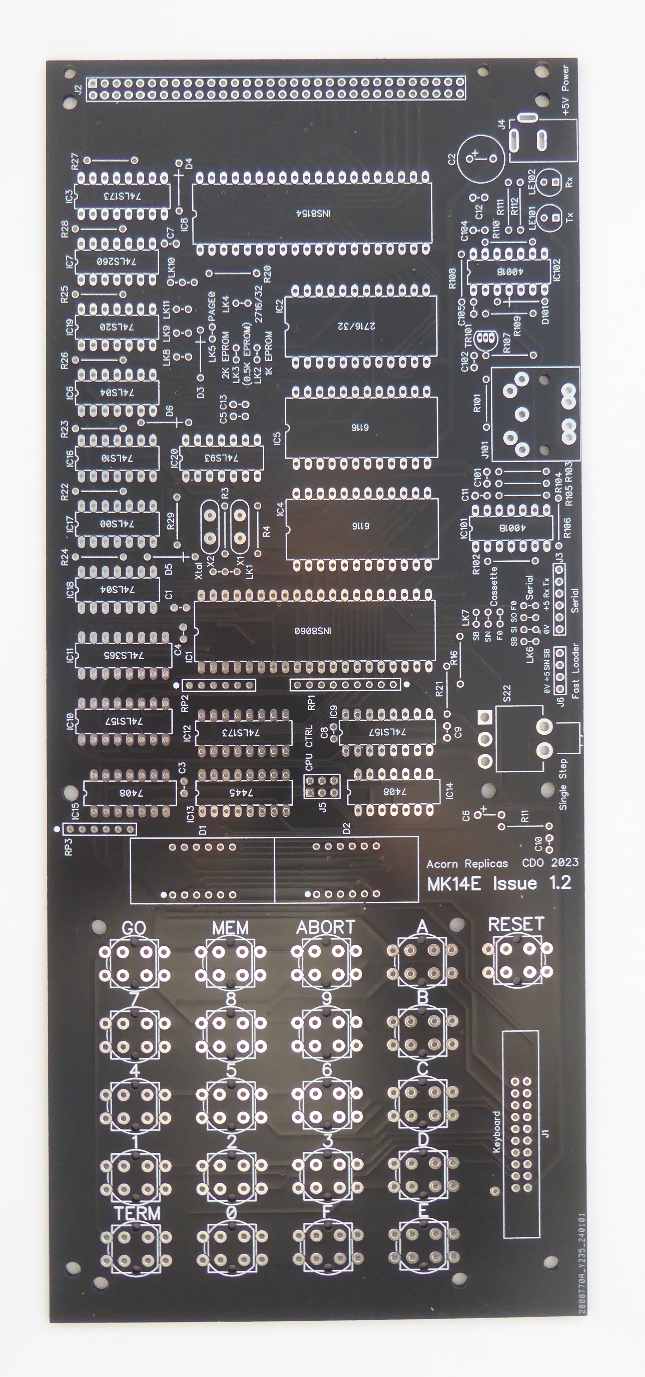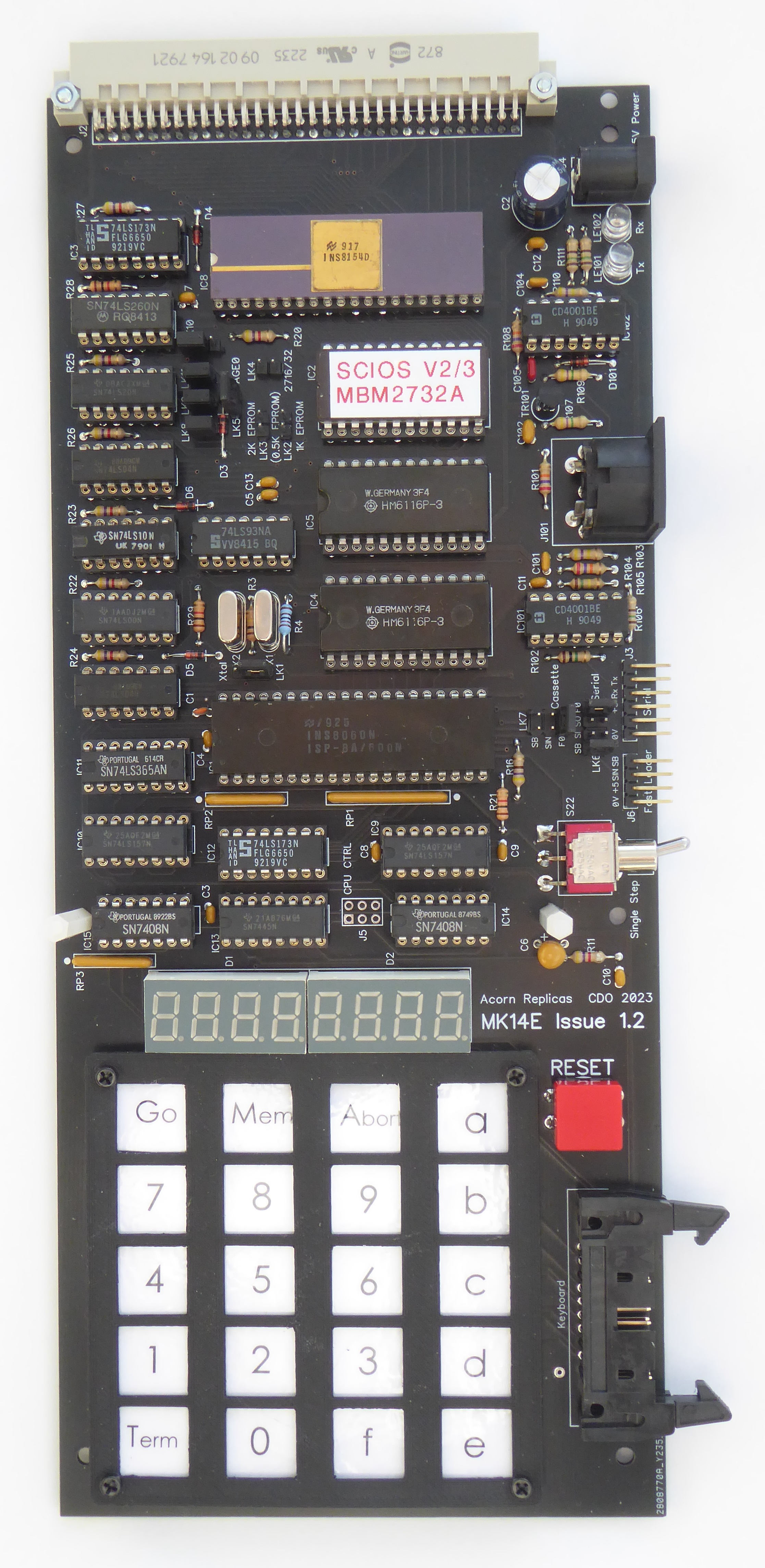
The MK14E Mainboard retains as much of the essence of the original Science of Cambridge design and maintains compatibility with SCIOS.
The memory devices, keypad and display have been upgraded to parts that are more widely available but still in keeping. The Single Step function and Cassette Interface which were originally add on PCBs have been incorporated.
CPU
The CPU (IC1) remains the original SC/MP National Semiconductors INS8060. The MK14 as standard was clocked at 4.433619MHz, if the VDU card was used then the crystal had to be replaced with a 4.0MHz which then meant the cassette interface timing was wrong, there is provision for two crystals which can be easily swapped between by changing link LK1 (not whilst running !).
The INS8060 internally has a 16-bit address bus but only 12-bits are brought out on pins, this limits the memory map to a meager 4K, IC3 latches the 'missing' four address lines allowing the whole memory space to be used. LK5 allows the on-board memory and I/O devices to be mapped into all pages (as original) or Page 0 when fitted.
Memory
RAM is provided by a pair of 2K byte wide devices (IC4 and 5) and ROM by a single byte wide 2K (2716) or 4K (2732) EPROM (IC2).
Links LK2 and LK3 allow for the selection of 512bytes (LK2 and LK3 omitted), 1K (LK2 fitted) or 2K (LK3 fitted) of the EPROM to be active. RAM IC4 will then fill the remainder of the first 2K of memory space.
LK4 is not fitted if a 2716 EPROM is used. If a 2732 is used then LK4 is normally fitted so that the lower 2K of the EPROM is selected, however by removing LK4 the upper 2K can be selected providing a convenient method for switching between two different 2K images e.g. SCIOS 2 and 3.
RAM IC5 fills the spaces around the I/O devices in the second 2K of memory space. This means you can have up to 3K of RAM plus the 128bytes in IC8 if fitted.
To allow off board I/O devices to exist in the Page 0 memory map pulling the EXT I/O line low (Backplane B7) disables onboard address access in Page 0.
I/O
With links LK8-10 fitted on-board I/O will be addressed at the standard addresses as in the original MK14 with no phantom images wasting memory space. If the phantom images are required (some software for various reasons uses the non-standard addresses) then removing the following links will put the images back:
LK8 normally fitted, remove to restore the 8154 image at 0A00-0AFF and 0E00-0EFF if LK9 is also removed
LK9 normally fitted, remove to restore the 8154 image at 0C00-0CFF
LK10 normally fitted, remove to restore the Keypad and Display image at 0900-09FF
Removing LK8-10 will give you a memory map with all the images present on an original V5 board.
The INS8154 at IC8 is optional, the board will function without it, if it is not fitted then removing link LK11 will fill the space with RAM.
The keypad uses modern tactile switches and the display high brightness LED's, there is provision for a QWERTY keyboard to be connected (via J1).
The keypad layout is the same as my replica MK14 so that a keypad overlay can be fitted as shown in the photo.
Links Summary:
| LK1 | Xtal | can be used to select between two crystals, usually X1: 4.000MHz (for VDU) or X2: 4.433619MHz (standard, for cassette) |
| LK2 | 1K EPROM | fit to use 1K of IC2 |
| LK3 | 2K EPROM | fit to use 2K of IC2 (if both LK3 and LK4 are removed then only 512bytes are used) |
| LK4 | 2716/32 | selects between 2716 (not fitted) and 2732 (fitted), with 2732 fitted can be used to switch between two 2K images |
| LK5 | Page | normally not fitted, fit to use the full 16-bit address space |
| LK6 | Cassette | connects SENSE-B, SIN and FLAG-0 to cassette interface |
| LK7 | Serial | connects SENSE-B, SIN, FLAG-0 and SOUT to serial connector as required |
| LK8 | 8154_A9 | normally fitted, when removed restores 8154 images at 0A00-0AFF and 0E00-0EFF if LK10 is also removed |
| LK9 | 8154_A10 | normally fitted, when removed restores the 8154 image at 0C00-0CFF |
| LK10 | KD_A10 | normally fitted in lower position, when fitted in upper position restores the Keypad and Display image at 0900-09FF |
| LK11 | 8154_CS | normally fitted, if IC8 is not fitted then removing this link will fill the space with RAM |
Connections
J1 Keyboard, the original edge connector has been replaced by a 2-part 3M style IDS connector, connections are as follows:
| Pin | Function |
| 1 | 0V |
| 2 | 0V |
| 3 | NRST |
| 4 | Column 0 |
| 5 | Column 1 |
| 6 | Column 2 |
| 7 | Column 3 |
| 8 | Column 4 |
| 9 | Column 5 |
| 10 | Column 6 |
| 11 | Column 7 |
| 12 | Column 8 |
| 13 | Column 9 |
| 14 | Row 0 |
| 15 | Row 1 |
| 16 | Row 2 |
| 17 | Row 3 |
| 18 | spare |
| 19 | +5V |
| 20 | +5V |
J2 is the DIN41612 Backplane connector.
J3 Serial, a 6-pin connector compatible with FTDI type serial-USB adapters, connections are as follows:
| Pin | Function |
| 1 | 0V |
| 2 | not used |
| 3 | +5V |
| 4 | Rx input |
| 5 | Tx output |
| 6 | not used |
J4 Power, a 2.1mm power jack for supply +5V power to the board (center positive).
J5 CPU Control, a 6-pin connector with additional CPU control lines that will not fit on the backplane:
| Pin | Function |
| 1 | 0V |
| 2 | CONT |
| 3 | 0V |
| 4 | NHOLD |
| 5 | 0V |
| 6 | NBREQ |
J6 Fast Loader, a 4-pin connector for connection to a Fast Loader (only from Issue 1.1 PCB):
| Pin | Function |
| 1 | 0V |
| 2 | +5V |
| 3 | SIN |
| 4 | SENSE-B |
J101 Cassette is a standard 5-pin DIN connector for connection to a cassette recorder, connections are as follows (same as original MK14):
| Pin | Function |
| 1 | Audio output |
| 2 | 0V |
| 3 | Audio input |
| 4 | Audio output |
| 5 | not connected |
Keypad
There are various options for the keypad:
'D6' style push switches
Omron Tactile switches (B3F-5050 with B3F-13xx keycaps)
Keypad overlay as shown in the photo at the top of the page (use 4.3mm high tactile switches)
The keypad overlay is avaliable from Ian Reynolds: 'Realtime' on the UK Vintage Radio forum or '55theparade' on eBay.
Mounting Holes
The board has a good selection of mounting holes for the keypad overlay and Eurocard as well as for general mounting:
Schematic
Bill Of Materials
Blank PCB