
Schematics:
Note: that there is a mistake on the schematic, pin 19 of IC9 & 10 it shown tied to 0V but should be linked to the enable signal on pin 1. This mistake appears to have made its way on to the PCB's as well. It is unlikely to cause a problem unless the bus request feature is used (B25).
Documentation:
for technical information see this section from the System 5 Manual System 5 Handbook Part 2 Section 2 6502A CPU Board [2]
Photos:
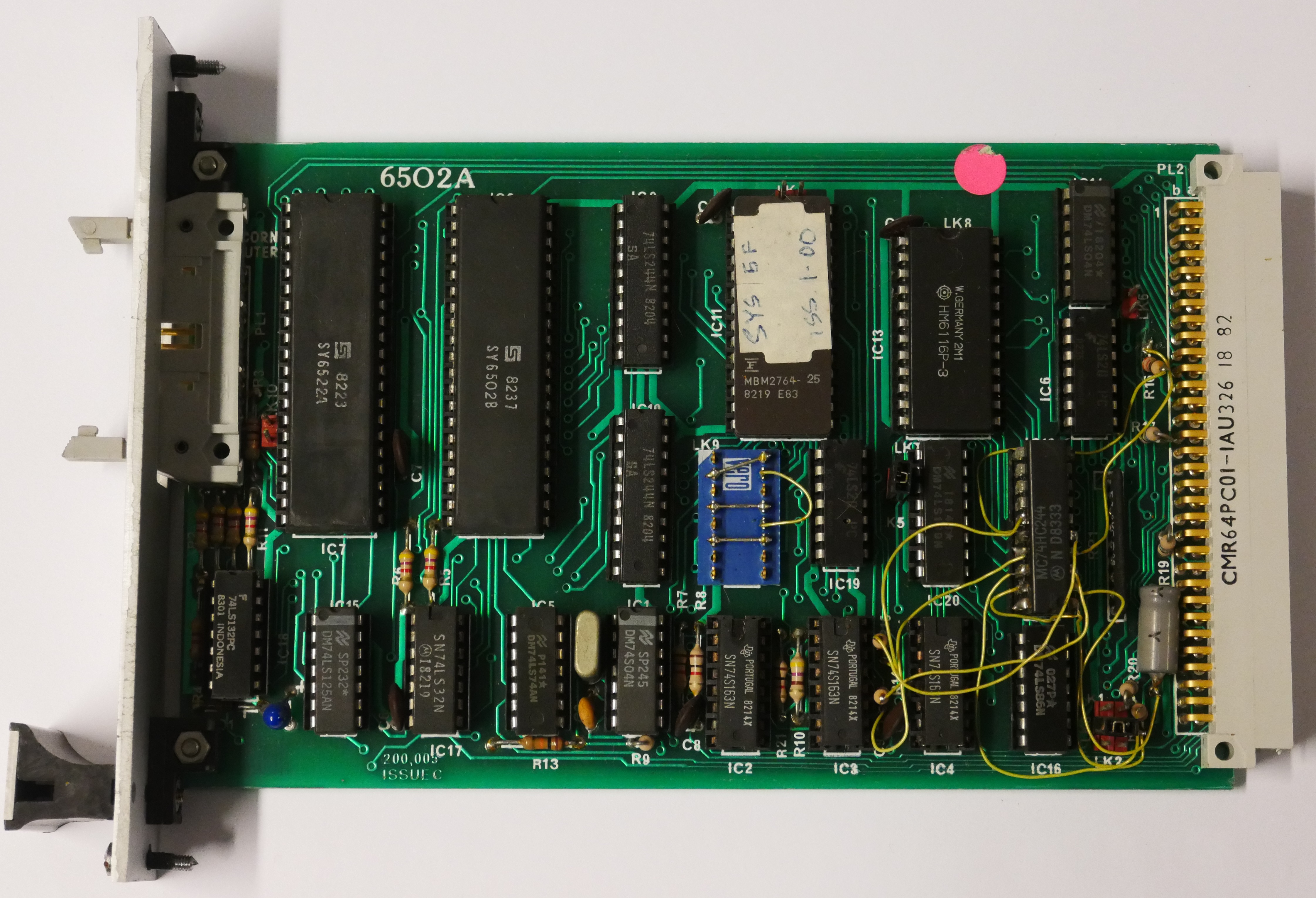
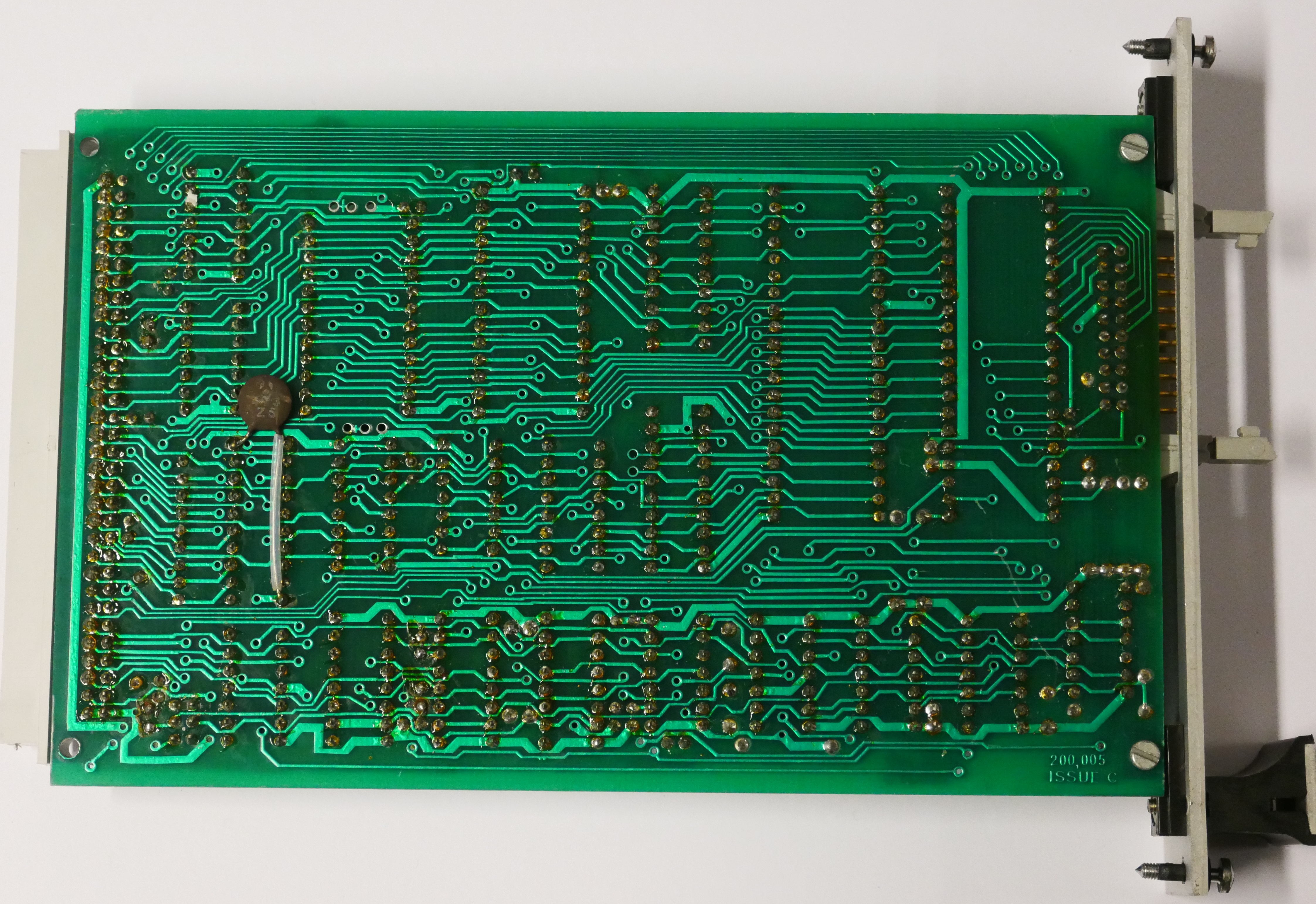
200.005 Issue C [3 System 5]


Data Sheets: