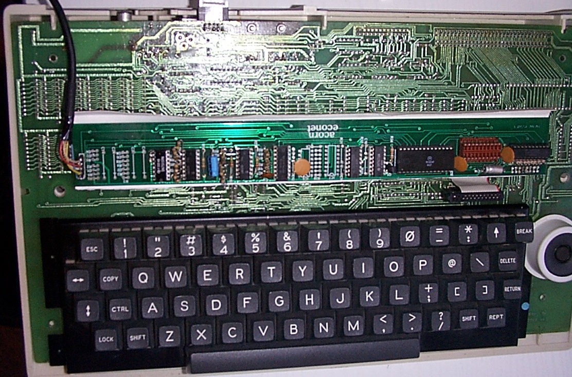
The Atom Econet Node connects to PL8 and fits inside the case, for this reason it is a long thin PCB that just fits along the top of the keyboard, a flying cable leaves the back of the Atom case and is terminated with a 5-pin DIN socket.

PL8 is strangely omitted from the Atom schematic, here are the connections:
| Pin | Function |
| 1 | D6 |
| 2 | D5 |
| 3 | D4 |
| 4 | NB400* |
| 5 | D1 |
| 6 | D2 |
| 7 | D3 |
| 8 | D0 |
| 9 | NMI |
| 10 | +5V |
| 11 | 0V |
| 12 | A1 |
| 13 | D7 |
| 14 | A0 |
| 15 | A3 |
| 16 | A2 |
| 17 | 1MHz |
| 18 | R/W |
| 19 | IRQ (via LK3) |
| 20 | NRST |
*active for $B400 to $B7FF (comes from IC49 pin 5)
As well as the Econet PCB an NFS EPROM must also be fitted in socket IC24 of the main Atom PCB.
Schematics:
I have found two versions of the schematic, Issue 2 includes clock generator and terminator circuits, these have been omitted on version 3. I have only found photos of Issue 1 and 2 PCB's both of which have the clock generator and terminator circuits present.
Documentation:
None?
Photos:
Atom Econet Interface PCB Layout Issue 1 [11]

Atom Econet Interface PCB Layout Issue 2[11]
